Rapidus 2 nanometers of production! Pat Gelsinger reminds: There must be unique advantages, otherwise it will be difficult to win the Taiwan power supply

Japanese semiconductor manufacturer Rapidus aims to achieve 2-nano chip production in 2027, and plans to accelerate the production cycle through fully automatic advanced packaging, competing with the crystalline foundry Longtou Tin Electric. However, in addition to improving production efficiency, Rapidus must show unique advantages in order to emerge in the fiercely competitive advanced semiconductor market.
According to the Japan Times report, Gelsinger responded to a question about Rapidus' potential at the Tokyo Journalists Association, "We appreciate Japan's efforts to promote the launch of Rapidus. But I also believe that Rapidus needs some fundamental differentiation technology. If you just try to follow the powerful NTD and do not have the breakthrough ability, this path will be very difficult."
Gelsinger is now a partner of the California investment fund Playground Global, and the company focuses on investing in new technology ventures.
Compared with other major wafer manufacturers such as Samsung, Intel and TEK, one of the advantages of Rapidus is a fully automatic advanced packaging that integrates automatic packaging and wafer processing in the same wafer factory to shorten production processes. However, this feature will not be enabled in the early stages, because the first stage area only provides crystal tests and does not have packaging test services.
Rapidus executive director Junyi Koike said that the company did not intend to compete with Taiwan Electric Power directly because Rapidus does not pursue super-large-scale production, which is Taiwan Electric's business model. Some customers want to obtain advanced chips tailored to their needs rather than general-purpose chips produced in large quantities, so Rapidus will focus on working closely with these customers to achieve expected results.
Rapidus aims to deliver the first sample wafers by 7 months and will provide early customer design tools to help them develop prototypes.
Gelsinger said that the United States and Japan are a powerful partner in promoting future technology and semiconductor industries. Part of the reason for Playground's visit this time is to meet with Japanese-related companies to help build breakthrough capabilities. As Japanese companies have a significant market share in the semiconductor materials, packaging and equipment fields, cooperation will bring development opportunities to new entrepreneurial companies invested in Playground.
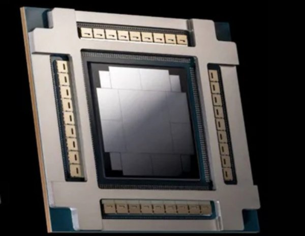
Rapidus has installed ASML's EUV (extreme ultraviolet light) and DUV (deep ultraviolet light) equipment in the crystal factory in Chiaki City, Hokkaido, and was installed at the end of last year. The company is also building the Rapidus Chiplet Solutions (RCS) R&D Center near Seiko Ipson Co., Ltd. next to IIM factory. The center will start preparing for the work from October 2024 and is scheduled to start installing equipment this month.
The R&D center will focus on the development of post-fab related technologies, including the improvement and redistribution layer (RDL), 3D packaging process, assembly design tools, and available chip (KGD) testing process.
Ex-Intel CEO Pat Gelsinger gives Japan’s new leading-edge chipmaker advice, says Rapidus needs unique tech to compete with TSMC Former Intel CEO Gelsinger has some advice for Japan’s Rapidus Extended reading: Samsung, SK Hynix CXL memory, due to insufficient demand for mass production card Meta poaches AI talents, OpenAI Taiwanese executive is surprised: It seems that someone is stealing something in his home