One of the keys to technological breakthroughs in GAA and CFET! ASM: Epictal technology has become an important role in advanced process
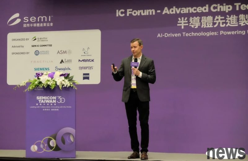
Glen Wilk, Vice President of Technology, Taiwan Advanced Technology, Dutch Semiconductor Manufacturer, Glen Wilk, mentioned in the SEMICON Taiwan 2025 theme lecture today (9th) that the Area Selective Deposition technology can effectively solve challenges in advanced processes, only deposition materials at designated locations, which helps improve process yield, component reliability and overall efficiency, and is suitable for advanced packaging applications such as 2 nanometers and below processes, heterogeneous integration, mixed bonding, etc.
This time, Glen Wilk, Vice President of Technology of ASM, delivered a theme lecture in the "Semiconductor Advanced Processing Technology Forum", sharing how ASM can promote chip manufacturing advancement 2 nanometers to EM, etc. through the ultimate precise control of atomic layer deposition (ALD) and epicenter (Epi) technology.
As demand for applications such as artificial intelligence and high-efficiency computing rises, global semiconductor industry is expected to exceed US$1 trillion in 2030, and chip architecture is accelerating its vertical 3D. Glen Wilk, Vice President of Technology at ASM, pointed out that 3D structures place higher requirements on the accuracy and thickness control of deposition processes, so ALD and Epi technologies will become keys that affect chip performance and reliability.
With GAA and CFETs, they have become the next generation mainstream architectures for logical processes. ASM’s ALD and Epi technology can provide atomic-level high precision, high uniformity and high ladder coverage material deposition in complex 3D structures, supporting high density and low power consumption transistor design.
Wilk emphasizes that epitaxial technology is the core of GAA components and plays an increasingly critical role in advanced logic production. In the FinFET era, the thickness of the channel flow in the transistor is determined by micro-shading and etching; when the GAA era, the channel is grown through the epitaxy process technology of atomic precision. ASM’s ALD and epitaxial technology not only drive the most advanced chip manufacturing today, but also the key to the continuous breakthroughs in GAA and CFET technologies.
Before 2028, the number of ASM employees grew by double digits, accelerating the layout of talents in TaiwanAt the same time, ASM has simultaneously accelerated the layout of talents in Taiwan, and is expected to grow by double-digit growth by 2028, and continues to expand investment in Taiwan to create more local employment opportunities.
ASM Taiwan General Manager Mu Bingcheng said that ASM is about to usher in its 20th year of deep cultivation in Taiwan. In the past five years, the team's scale has exceeded three times, and the offices are located in Linkou, Hsinchu, Taichung, Tainan and Kaohsiung, showing the promise of deepening its cultivation and close customers.
Jun Bingcheng pointed out that Taiwan is not only an important frontline for ASM's innovative technology, but also the core of sales and local services, and continues to support the key development of Taiwan's semiconductors from the 2-nanometer process to the Emmetre technology stage. From the beginning of this year to the end of 2026, we plan to add more than 100 new job vacancies. We sincerely invite more outstanding talents to join ASM to promote the global advanced chip manufacturing to a new generation.
ASM �
Extended reading: Aim at the challenge of advanced packaging! ERS Big Show Heat and Songkong Control Latest Solutions Integrating from heterogeneity to silicon photons, Sun Yuancheng: AI Super Moore and 3D×3D New Era